1 / 5
Ceramic substrates are ideal packaging base materials for new generation integrated circuits and power electronic modules. Compared with plastic and metal substrates, ceramic substrates have significant advantages:
1. Good Insulation: Ceramic materials are generally covalent bond compounds with superior insulation properties for high package reliability.
2. Low Dielectric Coefficient: Low dielectric constant and loss reduce signal delay and increase transmission speed.
3. Small CTE: High melting points result in a small coefficient of thermal expansion (CTE).
4. High Thermal Conductivity: Widely used in high-reliability, high-frequency, and high-temperature product packaging in aviation and aerospace industries.
| Item / Unit | 96% Al2O3 | 99.6% Al2O3 | ||
|---|---|---|---|---|
| Mechanical Properties | ||||
| Color | / | White | White | |
| Density | Drainage Method | g/cm³ | ≥3.70 | ≥3.95 |
| Flexural Strength | Three Point Bending | MPa | >350 | >500 |
| Vickers Hardness | Load 4.9N | GPa | 14 | 16 |
| Thermal Properties | ||||
| Max. Service Temp | ºC | 1200 | 1400 | |
| Thermal Conductivity | 25ºC | W/m·K | >24 | >29 |
| Electrical Properties | ||||
| Dielectric Constant | 25ºC, 1MHz | / | 9.4 | 9.8 |
| Volume Resistivity | 25ºC | Ω·cm | ≥10¹⁴ | ≥10¹⁴ |
Standard material for thick film circuit substrates. Features excellent electrical insulation, mechanical strength, and dimensional stability. Surface roughness: 0.2-0.6um.
Used primarily in thin film circuit substrates. Features higher purity, smaller grain size, and excellent surface smoothness (0.08-0.1um). Operating temperature up to 1700°C.
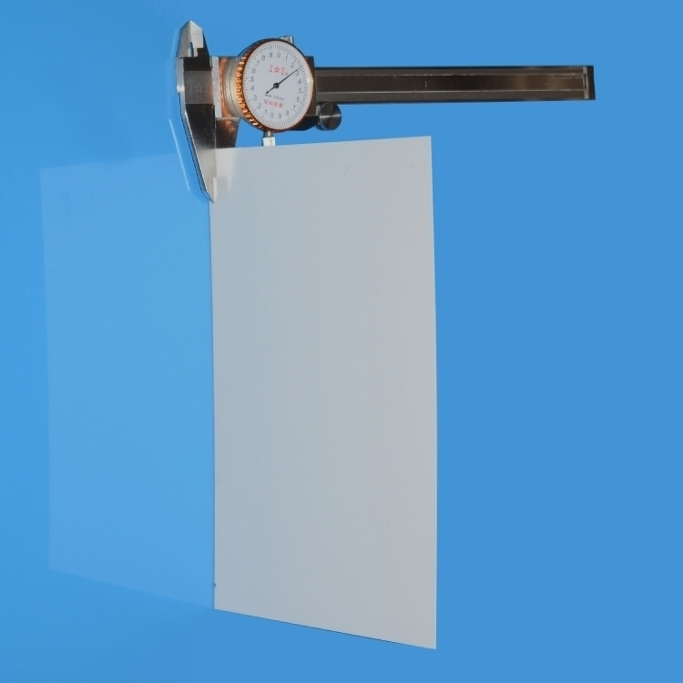
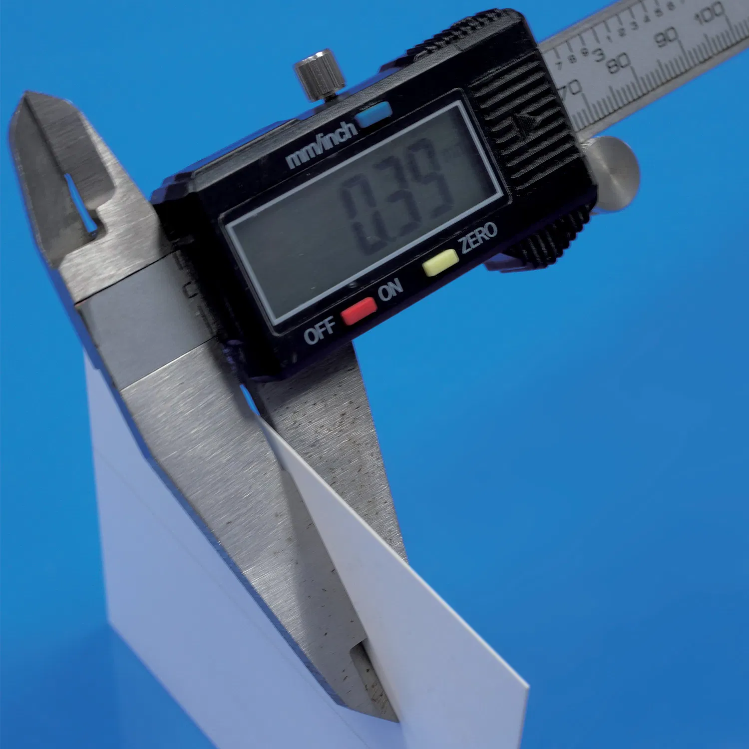
Standard Tolerances:
| Item | Thickness (mm) | Standard Tol. (mm) | Laser Cutting Tol. (mm) |
|---|---|---|---|
| Length/Width | / | ±2 | ±0.15 |
| Thickness | T<0.3 | ±0.03 | / |
| Thickness | 0.30-1.0 | ±0.05 | / |
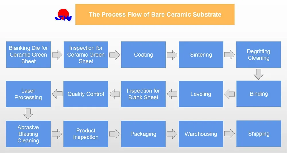
Production Process Flow:
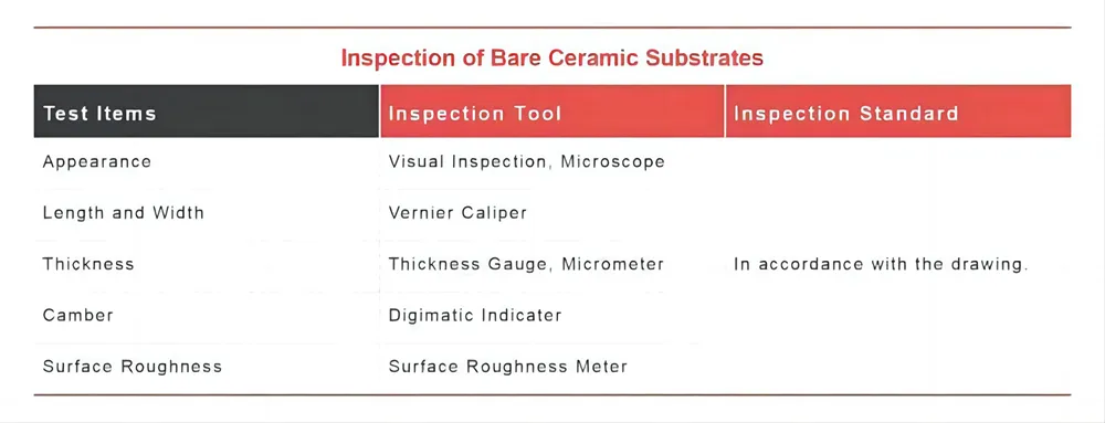
Quality Inspection:
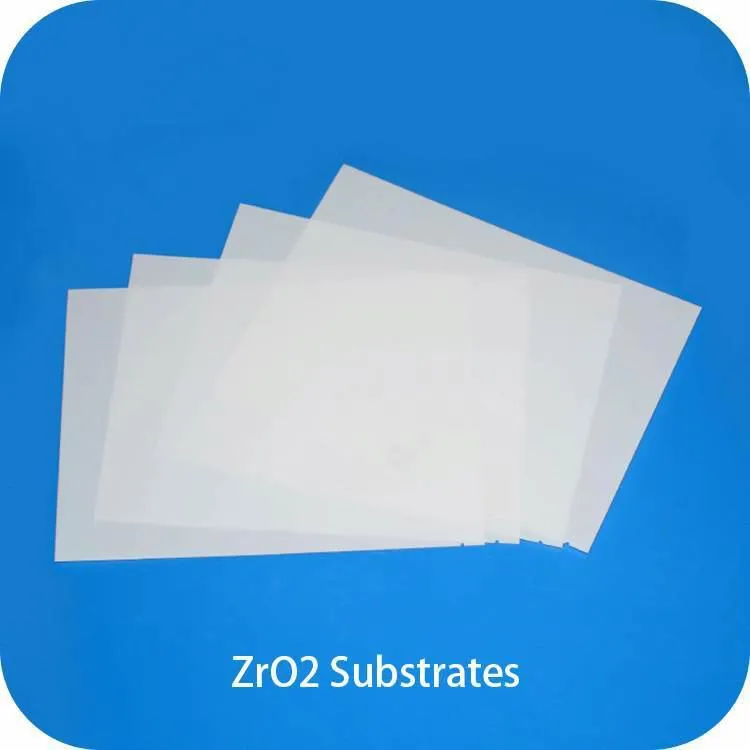
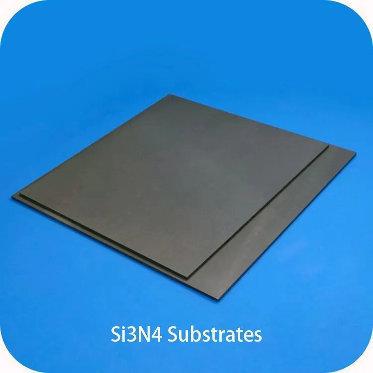
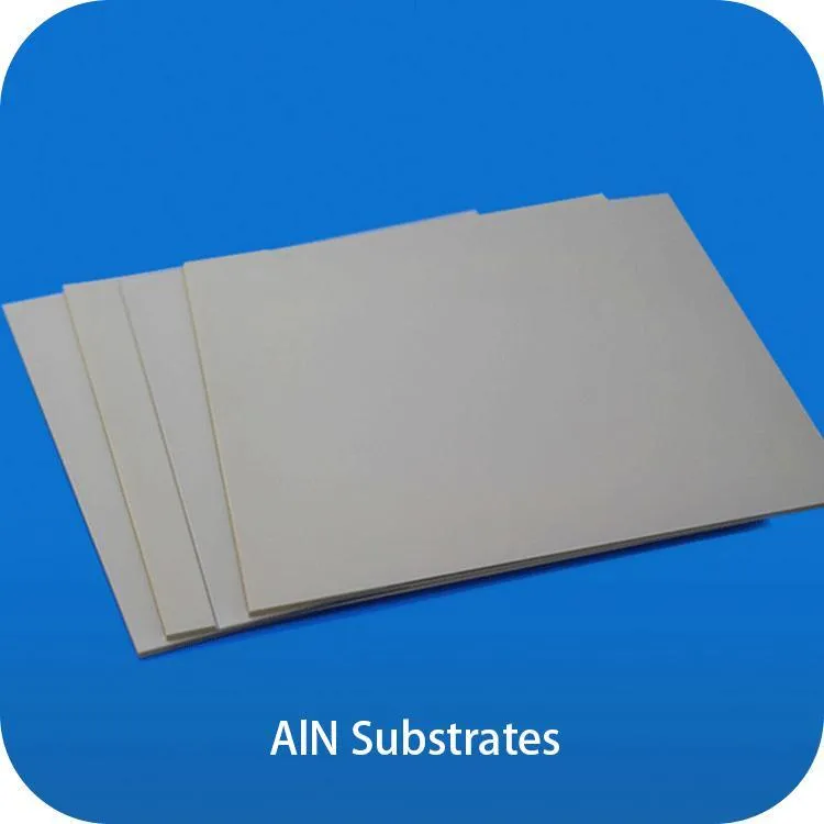
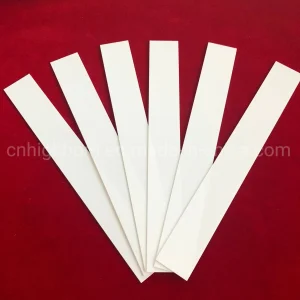
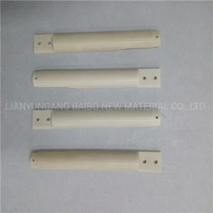
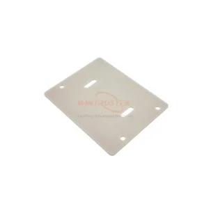
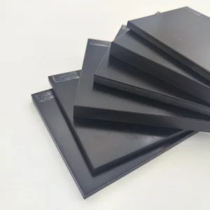
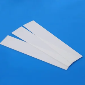
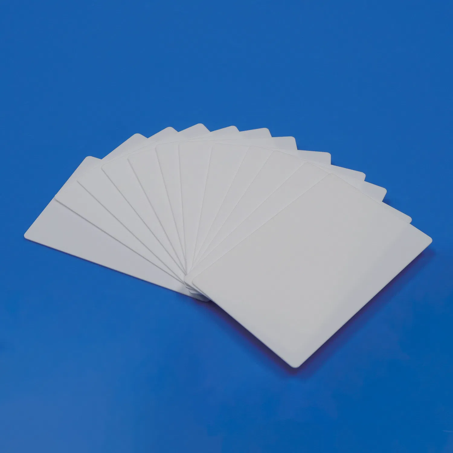
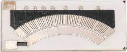
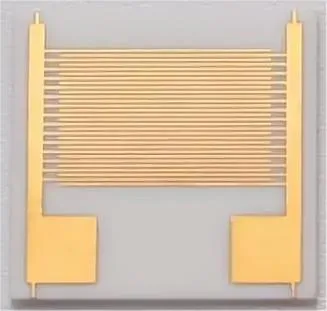
We offer bare ceramic substrates in various raw materials, sizes, shapes, and thicknesses.